IBM PS/2 Model N33 SX Type 8533 (PS/2 Note)
Yeah, IBM had some really snappy titles back before the Thinkpad.
N23 was a Japan-only machine and it's successor was developed as the N33 for the Western market. These machines are possibly the precursor to the Note 425 / Thinkpad 350 - possibly with a different hinge design - not necessarily how they're mounted to the chassis but the hinges themselves apparently instead of getting progressively stiffer to the extent they crack their plastic bases, they get looser and weaker - protecting the base but making the lid not stand up by itself.
They have an inherant flaw with one or two unique cylindrical fuses inside, one for the main battery and one for the AC. The N33 has a main power switch at the rea and another one on the front. If both are "on" and the machine still will not power up, then the notorious microfuse in the DC-DC converter is most likely blown. If either one is blown the system either it will run fine on batteries but not on AC and the battery is not charged or run fine on AC but not on battery.


I'll report back next week when I get some time with these machines but it would be interesting to note the design continuity between the N23, 33 and 45 through to the 425 / 350 which share a similar, but slightly evolved design
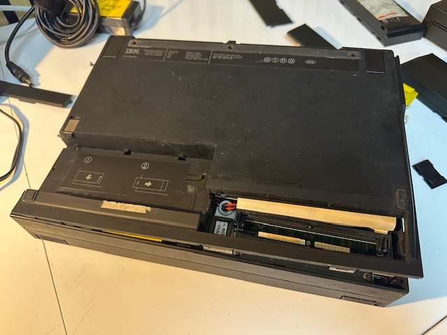
Teardown
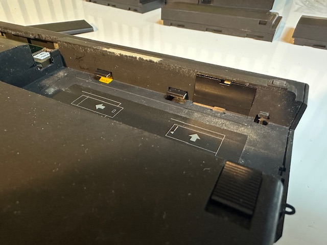
Intially I wanted to make sure there was no battery damage and check the fuses. You take the 3 obvious screws off the base and one side-ways on behind the main battery. You then push out this little door to reveal the clock battery, and remove it..
You then spudge your way around the base, where it will eventually pop off:
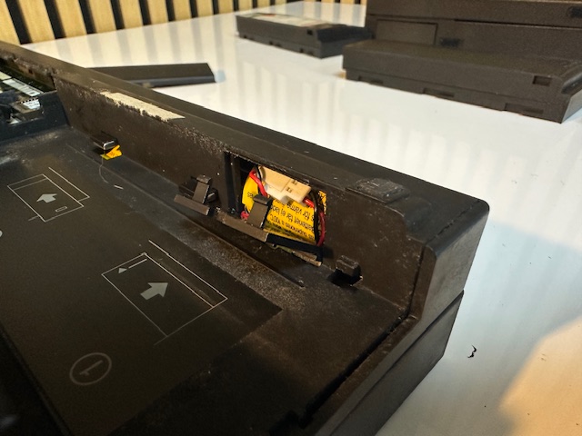
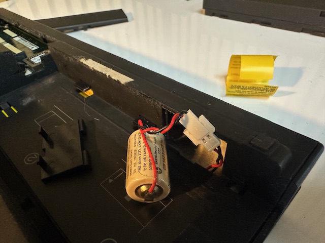
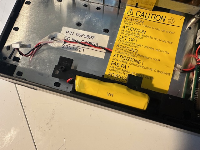
Revealing the deadly green hibernation/bridge battery. Remove it.
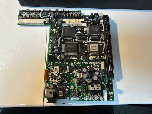
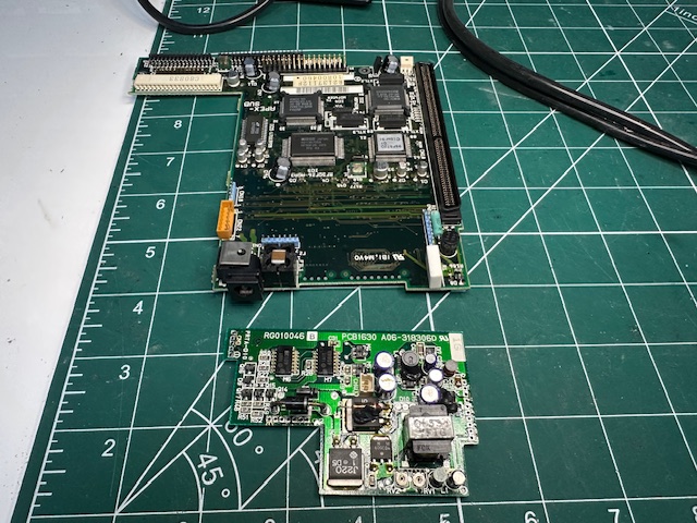
This next thing to take out is called the 'sub board' in the HMM and contains all 2 fuses along with a bunch of leaking surface mounted capacitors. It's a bit of a nightmare to pull out - it's held in place by 3 screws, a metal lever, 2 friction ribbon cables on the left, 3 battery connector cables and a bunch of drive attachments on both the left side and the bottom. You basically have to gently wriggle all around it removing it. It will eventually come loose.
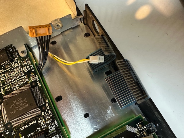
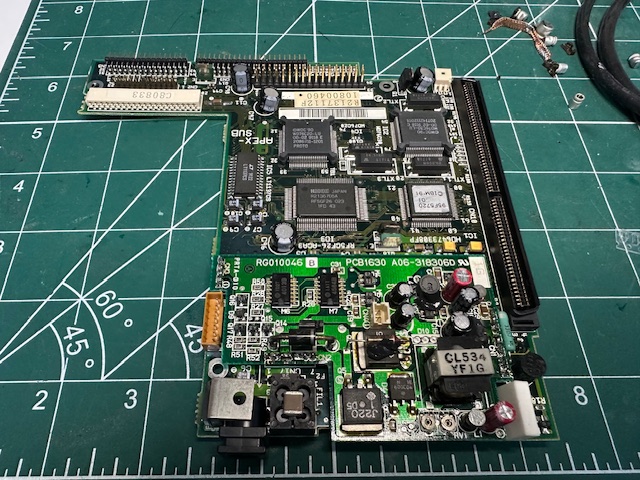
Here is the motherboard underneath:
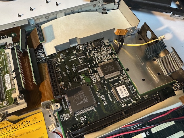
These two connectors are directly underneath the board with not a lot of space to pull them. The yellow one is (I think( for the lid detection - hibernate microswitch) and the other one possibly for the LED status lamps.
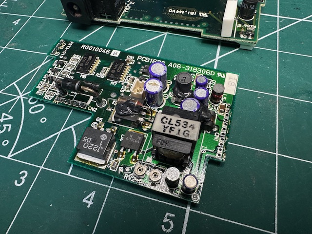
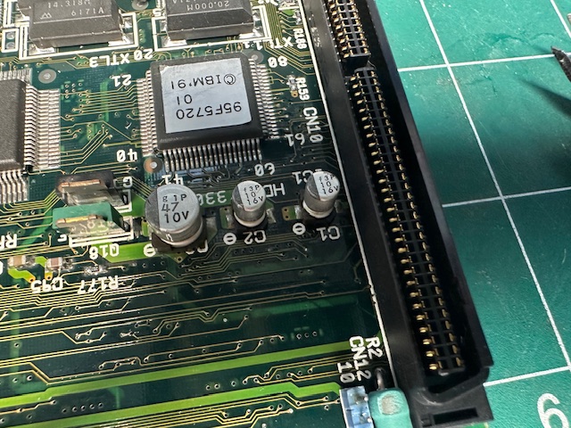
Now the hard bit - on the sub board that you have removed you'll find a daughterboard soldered on with a bunch of caps on. It's held in place by 3 soldered pin connectors, which you have to desolder to be able to remove the throughhole caps. On my removals, none of the through hole caps were leaking. Most of the surface mounted ones were.


This is the daughterboard removed. Note some of the connectors holding this daughterboard down have bridged pins. I don't know if this is intentional, but replicated the bridges when putting it back.
Here, where C11 was, it's possible the leaking electrolye had damaged some of the traces to the left of it. I can't be sure:
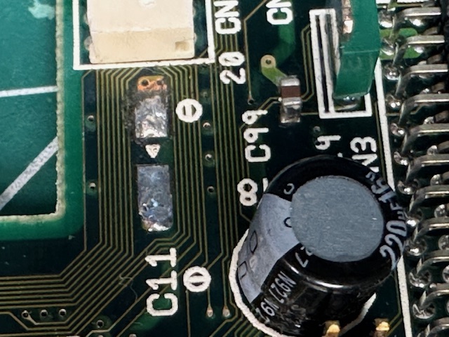
These three were definitely leaking:
And here is the recapped board, soldered back on.
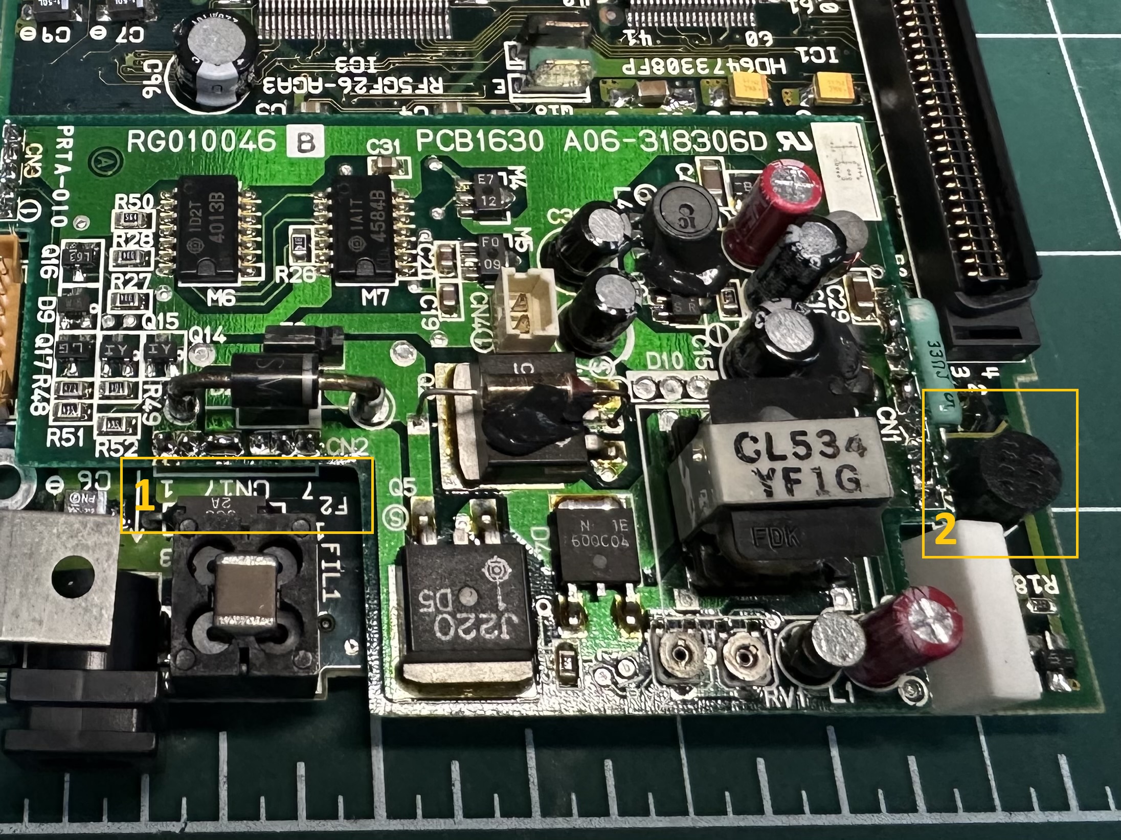
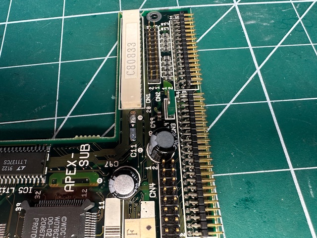
Below is a picture showing the two obvious fuses. 1 is the throughole 2a fuse. Mine initially was not blown and then because I think I had an iffy barrel connector, it blew. 2) there is a strange cylinder fuse on the right - which supposedly is for the battery. Mine had not blown.