I've got a few of these interesting transitional machines bundled away - and then someone alerted me that the elecrolytic caps leak and destroy the PCBs.... so back to the drawing board I go. Infact, this article contains a teardown of two machines. I remember when I did the first one I had the feeling there were two distinct motherboard revisions which indeed if you look closely between the first and second, there are definitely a bunch of updates.
It's also worth mentioning that in my (possibly later release) second machine, there was absolutely no cap leakage at all - so IBM must have gone with another manufactuerer.
Bit of background (bearing in mind a lot of history is in the wikipedia article) It's an IBM portable 386 machine from 1991 and was sold for $5995. It sits inbetween at least two flawed machines on IBM's journey to bring us portable personal computers, taking over from the 5155, Convertible and the P70/75 - each with their huge flaws but also delayed beyond it's useful life so much so it was released the very same month as IBM's original black 'PS/55 note' true notebook computer which althought it had it's own flaws, at least it was truly portable. This machine compromised size for a full travel, full-sized 'proper' keyboard, which was something IBM later brought to the notebook market convincingly with the Thinkpad 700C, but couldn't make up for this machine's other difficiencies.
Yes the keyboard is wonderful to type on, but if this machine is basically tied to the desk, why wouldn't I be using a much cheaper desktop computer with a proper display?
At the time of it's development, IBM USA had all these out-dated ideas about how the design must conform to age-old colours, designs, naming conventions, testing and were pitting various different design and manufacturing outposts against each other. This brought us a bunch of fabulously varied, but all flawed machines, mostly with silly alpha-numeric names and in many cases unrelated to one another, until we get to about the 750 era where all the crappy ideas (hinges, displays, architecture) were gone.
The L40 SX is part of that journey and is actually one of the nicer ones to own. Having said that, I couldn't help but think the hinges on this thing are going to get a bit achy in another few decades....
It's also worth nothing that whilst the L40 SX lacks the branding, the pointing solution, the high-contrast colour screen, the speed, the portability it did serve as a useful testbed for various other 'killer app' hardware designs which would make a huge difference later on. There are prototypes in black, with TFT colour screens and with the 'pointing stick' which became the Trackpoint II. Sapper famously disliked this machine but perhaps it's existence as a stick to beat IBM executives over the head with did help in the long run. They couldn't KEEP getting it so wrong.
Anyway, back to the point. I learned this (first) machine sits right in the middle of a 'crap capacitors' epidemic - somewhere between the mid-80s to mid-2000s, where electrolytic capacitors (little cyclinders of fluid on PCBs) fail and leak. The fluid inside rots everything it touches and destroys it. You can either replace them with new ones which hopefully won't ever leak or, in some cases Tantalum capacitors which are solid-state and when they fail they just sort - annoying but not destructive. In order to start preserving mine, I decided to pull one out and tackle it blind.

It was unclear as to how many capacitors there were so I was going in blind. I've seen images of the motherboard with a certain green capacitor on the bottom-left hand side, near the left memory slot which always seems to leak and mine didn't have it or even have a lot of chips in the same spot, so definitely more than one revision - bear that in mind when looking at my notes.
This machine is fairly easy to get at and the only issue really is that the cream plastics are getting a little brittle - especially around the hinges on the LCD bezel. So take your time.
If you take the 3 screws out of the bottom/front, you can lift up the keyboard and carefully remove the two ribbon cables which are simply push-fit. This shows the front half of the motherboard. The back half is obscured by the plastic panel which has the power switch and all the LCD indicators in it, which is removed by 3 screws on the back and about 4-6 on the front, under where the top of the keyboard was. This then lifts off to show the whole motherboard. Which, I think is an early revision of this machine. See the next machine further down to see the later one.

It's also now worthwhile to completely remove the lid, which is attached by the hinges which have 2 screws either side, also removed from the rear. You need to unplug 2 cables on the left and 1 on the right and then the whole lid and hinges slide vertically off.
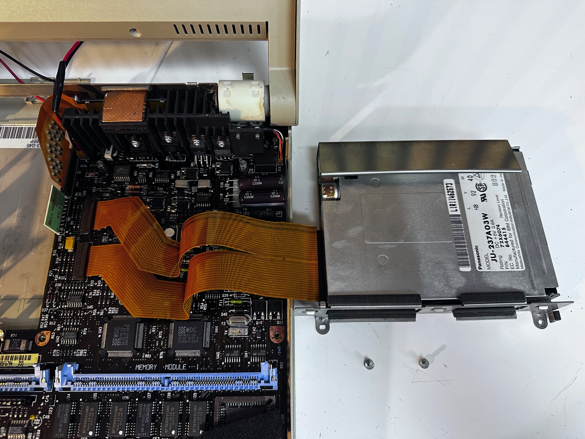
Now you have the mainboard accessible, you have to remove the HDD, the centre plastics around the main battery and the FDD - all of which are a few screws and ribbon cables.

On my motherboard, there were 6 x through-hole electrolytic caps on the left which showed no signs of leakage, but I replaced them. For some reason, IBM covered the legs in which flaky white gunky glue stuff. It's dry and doesn't seem to do any damage but it does get in the way. I removed all the stuff which was around the caps and cleaned with IPA on both sides before installing the new ones.
C183 - 220uf/10v
C184 - 120uf/25v
C233 - 120uf/25v
C234 - 120uf/25v
C222 - 820uf/25v
C221 - 1500uf/10v
The mainboard has a substantial copper backpane which sucks up heat. I would strongly suggest you use a hairdryer or gun to gently warm the whole board before you start. I didn't have any trouble but then again I have a very expensive desoldering gun.
Next we move onto the LCD, which is mostly held on with friction. You remove 2 black screws from the bottom and then you have to work the LCD bezel free by gentle prying the outside of the lid away from the edges. It's nerve-bending but not too tricky.

I help update the thinkpad TFT wiki to try and make it easier to source replacements when you need them for LCD screens. My focus tends to be on older machines, so it's not just TFTs in the main list now and whilst there are still voids in what it notes (seen where it groups together a bunch of different machines which do not, infact share the same screen), a lot of them are now correct.
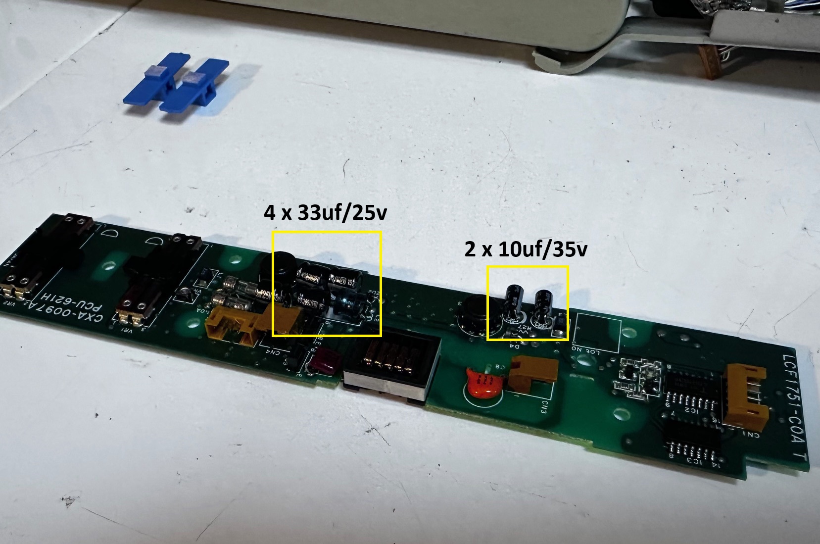
Inside the LCD is the inverter, which comes out with 4 screws and is relatively easy except the 6 capacitors on it are very very shallow.
C1 - 33uf/25v
C2 - 33uf/25v
C5 - 33uf/10v
C11 - 33uf/10v
C13 - 10uf/35v
C14 - 10uf/25v
I didn't have small enough capacitors so I had to be creative and right-angle them with some electrical insulation around the legs. Note the close up of C1/C2 shows how absolutely rotten they were underneath (although on this journey, these and C5/C11 slightly, were the only caps I found to have leaked - I think as I have a slightly later-release motherboard, my mainboard caps were not of the same flawed design as some other L40SXs)

This is my inverter after replacing with less-than-ideal-but-perfectly-fulfil-the-job capacitors:

Finally there is the LCD itself which is the highest-risk change. I actually think all these caps were good and didn't show any signs of leaking, so if you're a gambler, I would maybe leave these 7 caps. They're actually fairly easy to remove but getting to them is a pain. You have to remove 4 screws holding the LCD down onto the lid and then you can unplug all the cables and then fold over the LCD 180 degrees sideways onto your bench, revealing the backs of the capacitors. There is a bit of plastic insulation stuck over the top which you would either peel off or cut a small piece off to get access to the bottom of the capacitors. I cut mine, below. They're simply 7 x 10u/35v through-hole capacitors. There is a fair bit of room above them so you can generally afford to go a little bigger if that's all you have. Mine were much bigger and the whole thing went back together with no problems.
Before, with the LCD unscrewed and turned upside down:

Here are my new, slightly bigger caps attached:

I was so relieved when I plugged the lid back in to test and there were no dead lines. I've found the thin wires which run all along the side of the LCD panel to the PCB can really easily get damaged and die/short. The key is to go gentle and try and get in and out quickly, once and with the least amount of movement possible.
Not-Capacitor Related..
A few people asked me about my L40 SX just to get a few more bits of info.
Drives - the floppy on this one is a standard 1.44Mb 3.5" IBM-compatible drive and works fine without any service so far. Which is very useful because the original IDE hard drive was dead. I have opened up some other L40SX machines which did not have any signs of having a hard drive, so I think some may have not come with them. I replaced my hard drive with a Compact Flash card and a 2.5" IDE->CF card, with MS-DOS 6.22 and Windows 3.11 - all installed from the original floppy disks. I did this a few years ago but I don't remember any issues. I simply booted using the MS-DOS installation disk 1 and F3'd out to do an FDISK on the CF card. This set it to a simple FAT16 parition and setup the MBR fresh for this machine/disk combo. After formatting, I simply installed MS-DOS 6.22 as usual and then followed up with Windows 3.11.
Numeric Keypad - I have acquired a few L40 SX machines over the years and a few of them came with this keypad. I don't know if it was originally included or was an optional extra, but it's very nice and I think fairly rare. It connects over some kind of unique RJ-45 cable (like the ones you get on ethernet cables).
Keyboard - Yes it feels nice. It's a bit soft for my liking and I think some people think it's some kind of weird Nirvana of a keyboard because Nostalgia Nerd on youtube did a video saying how amazing it is. It's fine.
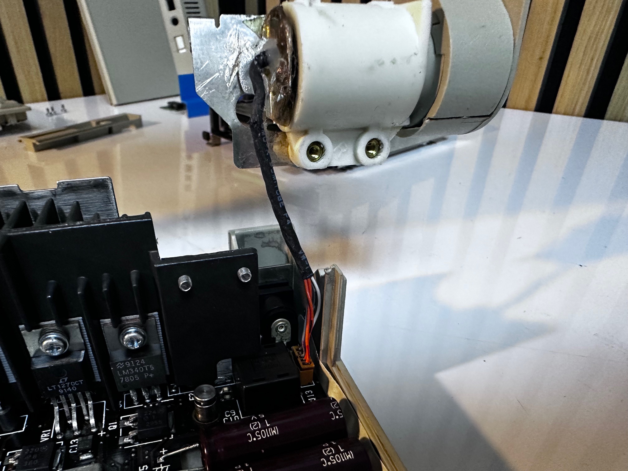
Preservation - make sure you remove the main battery, even if it shows no signs of leakage. From distant memory there might also be a hibernation battery towards the back of the machine which also can leak and corrode everything around it with horrible fumes. Take both out and seal them up in an airtight bag if you want to keep them.
PSU - no doubt the external PSU 'brick' also has some high and low voltage capacitors in it, but I've got more important things to tackle than that.
The second machine...
Ok, so I had another machine in this unique carry case. I did a bit more note-taking as I took it apart, so here we go:

Flip the machine over and remove the 3 covered screws:


Lift up the keyboard at the front and slide forward, then remove the two friction-held ribbon cables from underneath.


Remove the 3 top screws at the back which sit over the cream plastic brackets

Lift forward the LCD indicator bezel and flip over to remove it's two clipped down ribbon cables:

Remove the floppy drive's 2 screws along the front, lift up and then unclip the two ribbon cables for the floppy drive
Finally, to break open the display you need to remove the screen. This is held in by two block connectors on the left and 1 connector on the right and then undo the 4 screws holding the hinges in at the back.

Here is a picture of the inverter, which on my second machine had the same layout and 6 capacitors but zero rot.
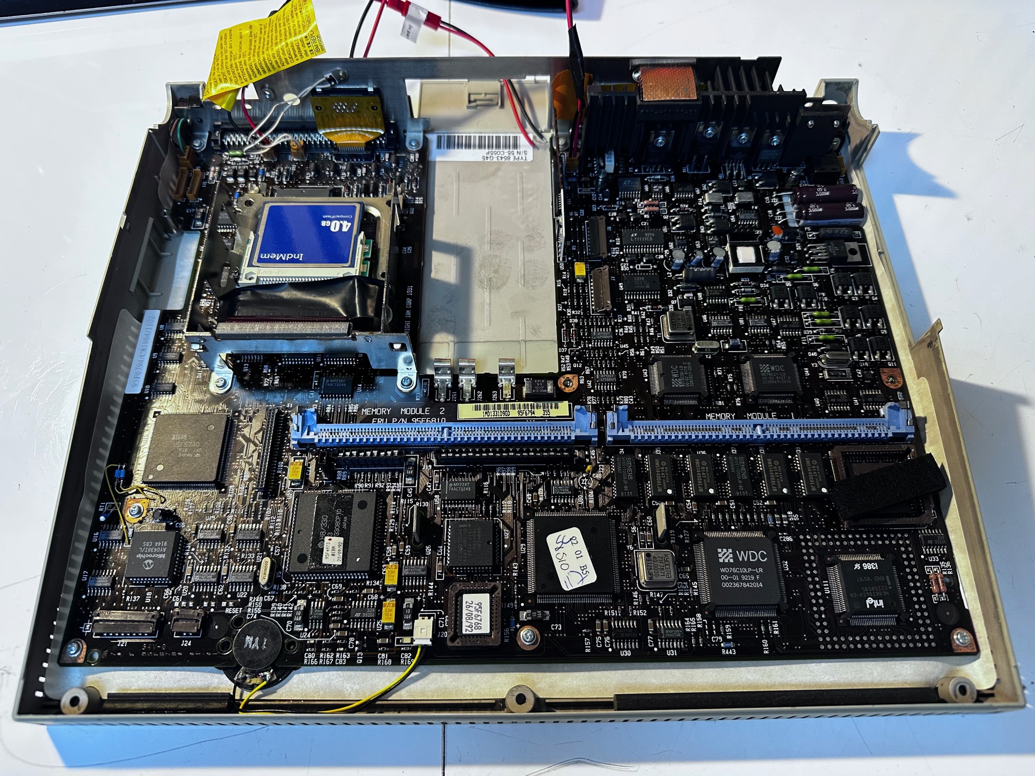
For those looking to compare motherboards, here is a picture of my later machine's motherboard:
And finally, some uber-cool images of the machine laid out with it's special reversible mouse/trackpoint 1, expansion keypad and custom carry case with Kodak printer.


For fun I lined 1991's L40 SX against 1992's CL57 SX and if you look closely, considering they reach evolved from very different spaces, you can spot a lot of similarities:


