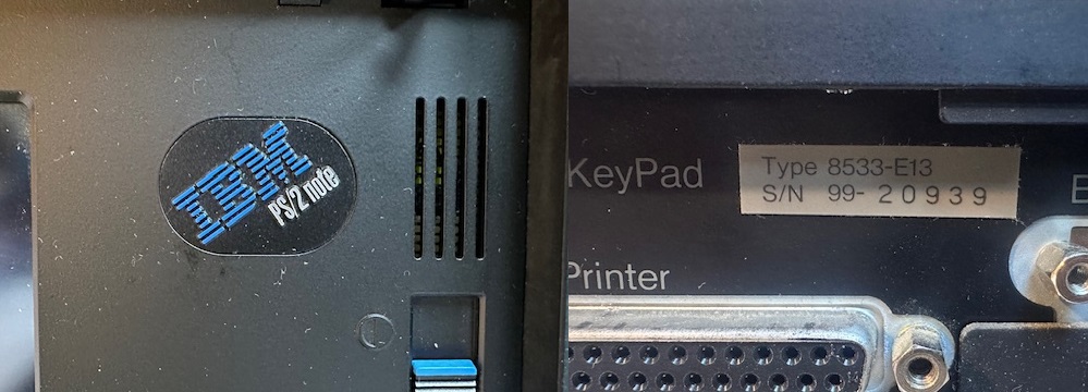
N33 is derided from the 8533 Model Type. Yeah, IBM had some really snappy titles back before the Thinkpad.
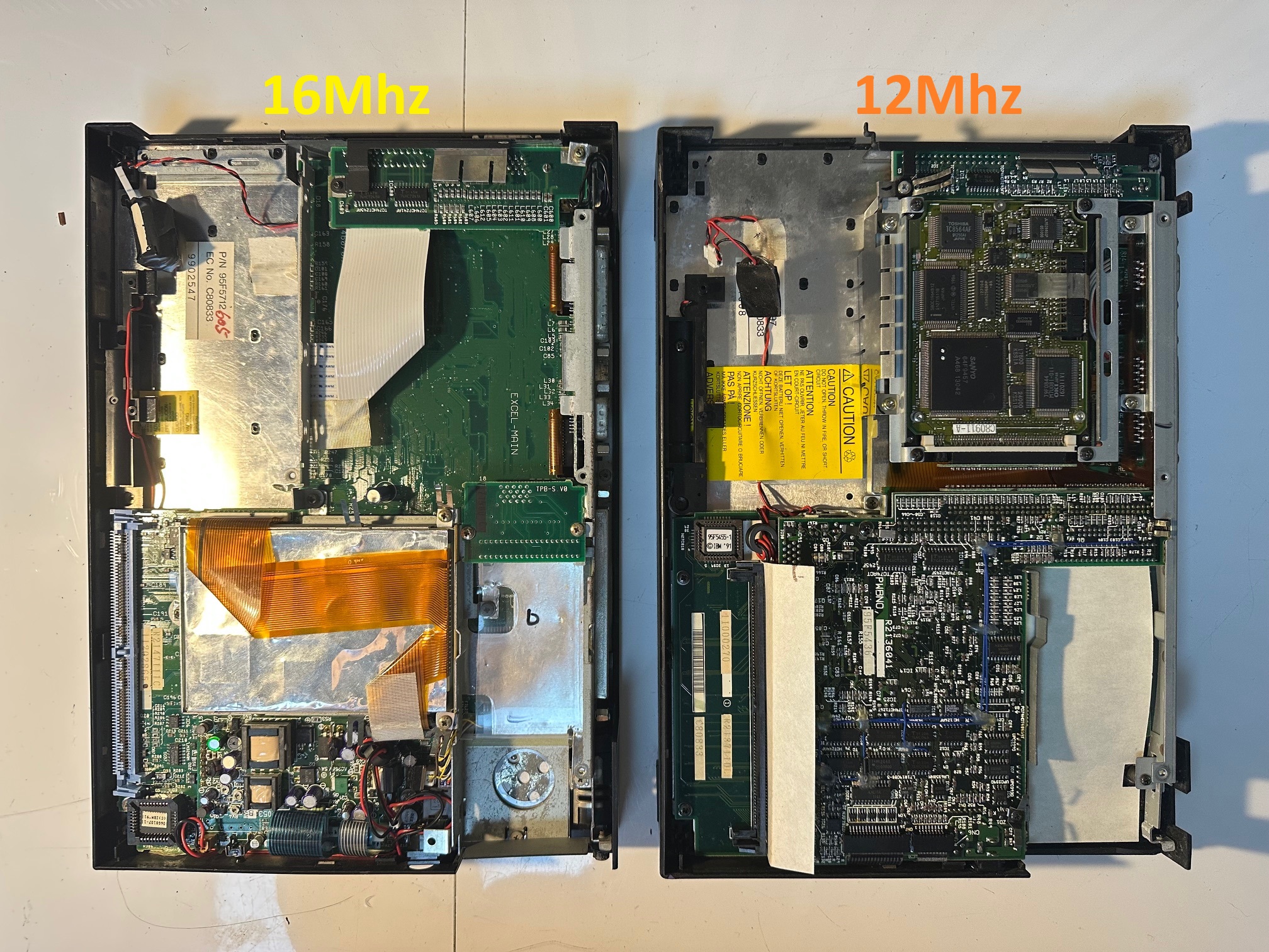
Note: this article is about the 12Mhz 386 model which was seemingly derived from the first generation PS/55 Note, whereas the 16Mhz version was derived from the second generation PS/55 Note which was called the N23 SX. Inside it's a completely different motherboard to the 16Mhz with no external display, no invert display switch and no built in floppy because the two-part construction of the main two boards leave no room for the Hard Drive to mount on top of them - therefore it's moved to take up the space of the floppy drive. I believe it was an option to have either a HDD or a FDD and my one has the HDD option with FDD connected via the external connector.
| Model | IBM PS/55 note N33 SX |
| Machine Types | 8533 |
| Release Timeframe | Sold from April 1991 |
| Preceded by | IBM PS/55 note and N23 SX were the Japan-only siblings, released earlier than the international N33 SX models |
| Superceded by | N51 |
| Motherboard Specs | 12Mhz 80386 |
| Display Specs | 9.5" Monochrome display with 640x480 |
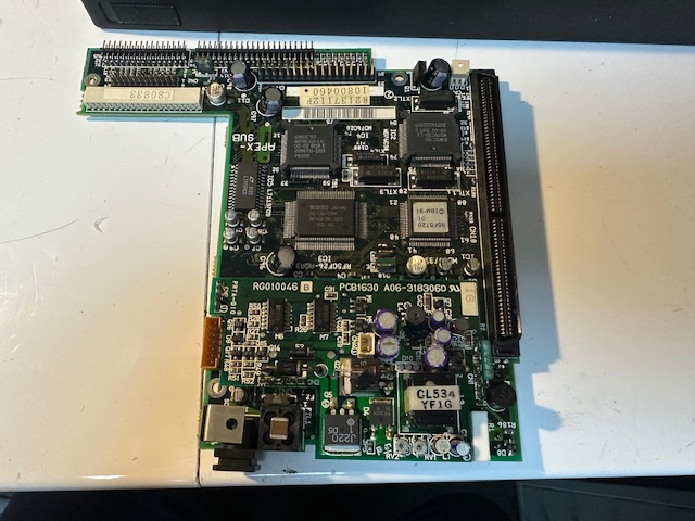
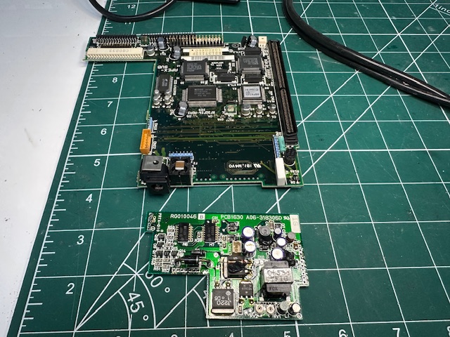
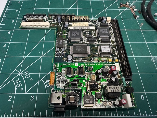
The dual-planar design mainboard PCBs inside are codenamed APEX-MAIN and SUB-BOARD
The N33 machines are successors to the original note and N23 SX Japanese machines and is a precursor to the N51 and C23V Notes - which eventually became the C52 Thinkpad 700C. They're ISA bus.
They have an inherant flaw which revolve around the fuses inside, one for the main battery and one for the AC. Both N33 machines have a main power switch at the rear and another Standby switch on the front. If both are "on" and the machine still will not power up, then the notorious microfuse in the DC-DC converter is most likely blown. If either one is blown the system either it will run fine on batteries but not on AC and the battery is not charged or run fine on AC but not on battery. I've also found the barrel connector can suffer from corrosion and you need to 'rub' the power connector in and out to get a good connnection for the 15V DC.
Here is a picture of the 16Mhz model on the left and the 12Mhz model on the right. The 16Mhz is mainly one large motherboard which is the same as the Japanese PS/55 Note N23 SX, whereas the 12Mhz model is two equally-sized boards connected together the same as the PS/55 Note (1st gen). Due to this 'fatter' construction of the main two boards, the hard drive cannot sit directly on top and is moved into the void where the internal floppy drive sits on the Japanese N23 SX machine.
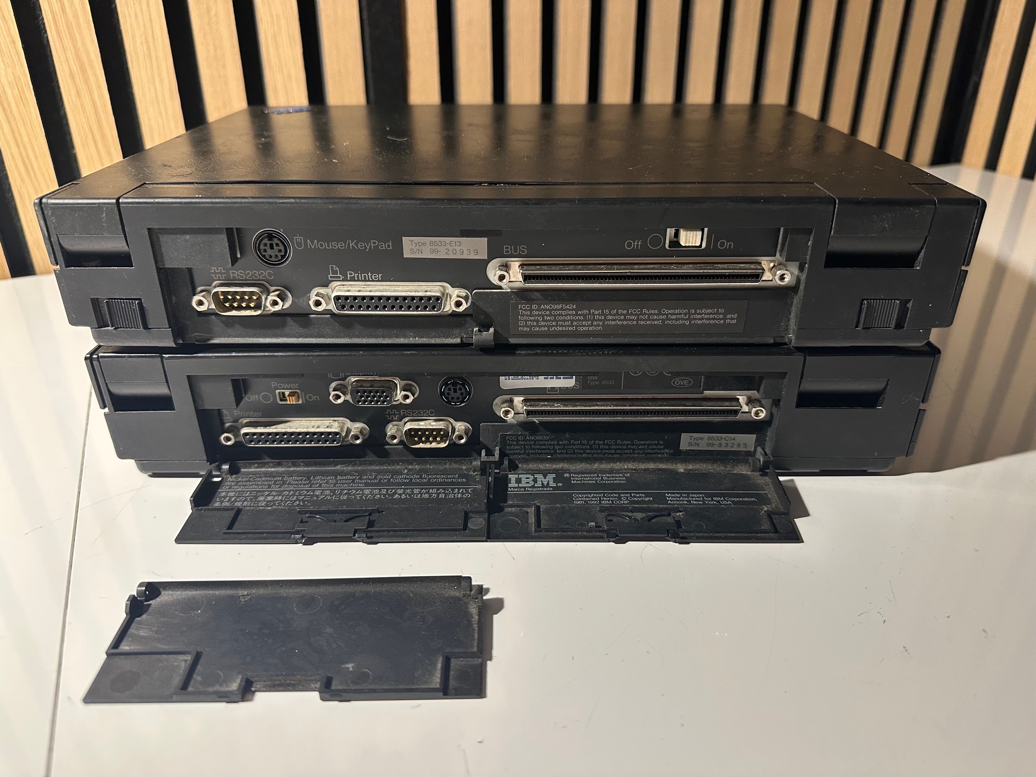
Also here is a picture showing the 12Mhz without external display output and 16Mhz model with external display output:
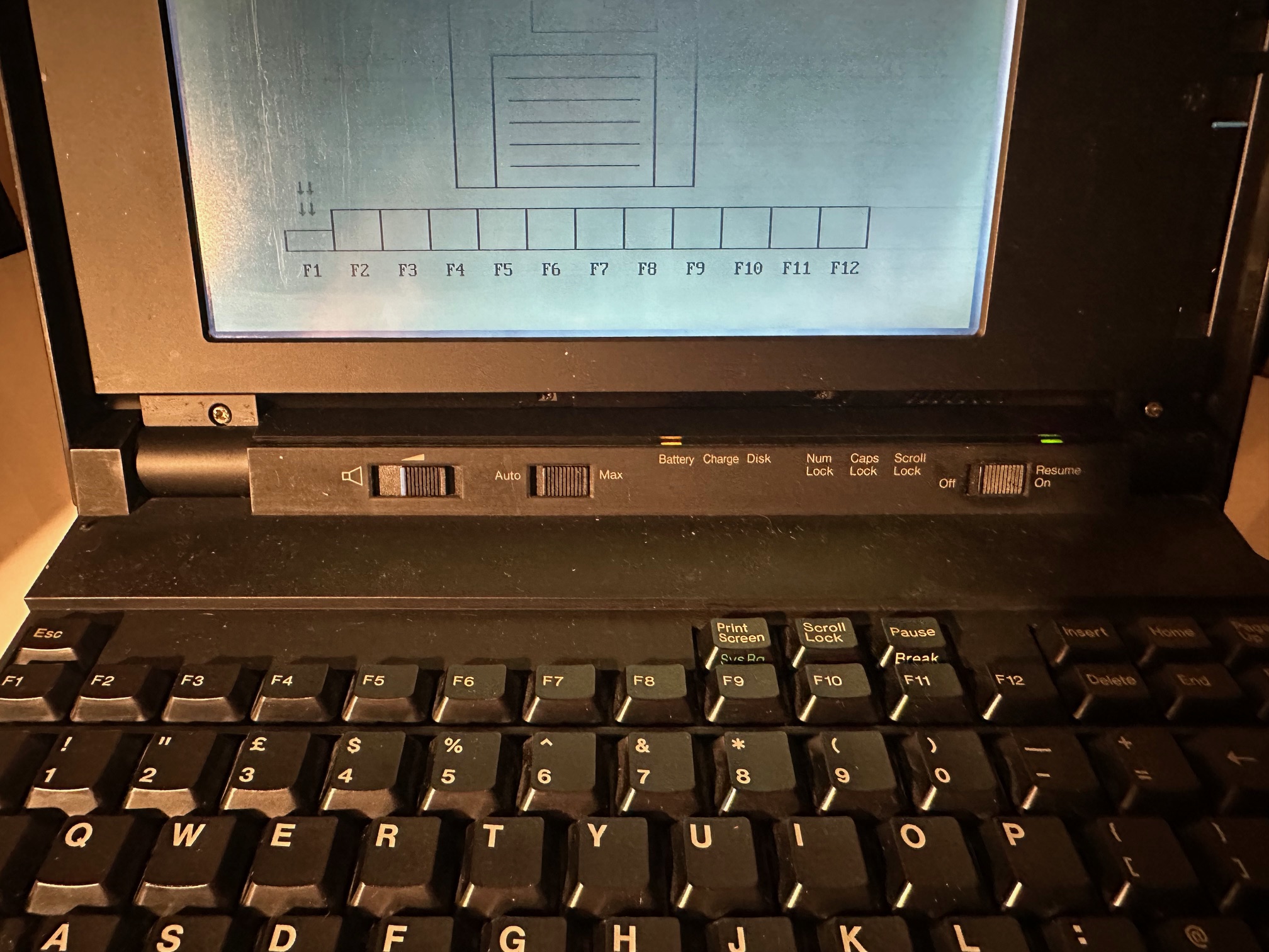
Another clue on the outside is that the 16Mhz has an 'invert screen' switch which will flip the monochrome display from light to dark. This is not present on the 12Mhz.
The 12Mhz model LED bezel without the invert switch:


I'll report back next week when I get some time with these machines but it would be interesting to note the design continuity between the N23, 33 and 45 through to the 425 / 350 which share a similar, but slightly evolved design
N33 SX 12Mhz Teardown
Intially I wanted to make sure there was no battery damage and check the fuses. You take the 3 obvious screws off the base and one side-ways on behind the main battery. You then push out this little door to reveal the clock battery, and remove it..
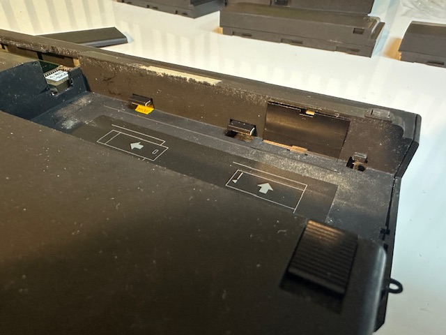
You then spudge your way around the base, where it will eventually pop off:
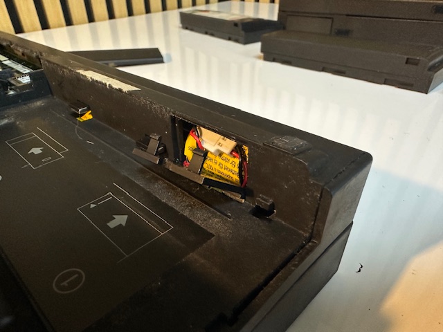
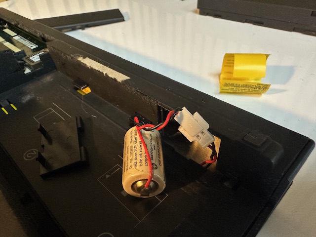
Revealing the deadly green hibernation/bridge battery. Remove it. The machine can no longer recover from going into standby but at least it will not corrode itself to death when this battery leaks.
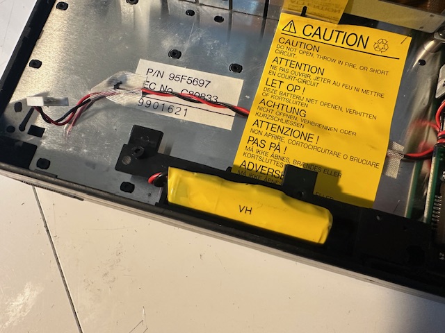
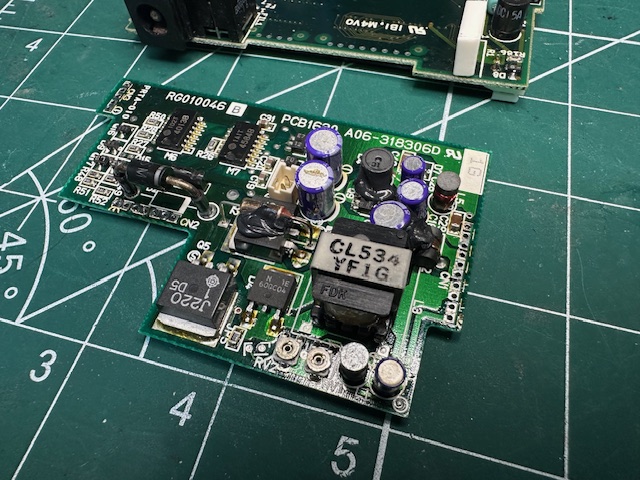
This next thing to take out is called the 'sub board' in the HMM and contains all 2 fuses along with a bunch of leaking surface mounted capacitors. It's a bit of a nightmare to pull out - it's held in place by 3 screws, a metal lever, 2 friction ribbon cables on the left, 3 battery connector cables and a bunch of drive attachments on both the left side and the bottom. You basically have to gently wriggle all around it removing it. It will eventually come loose.
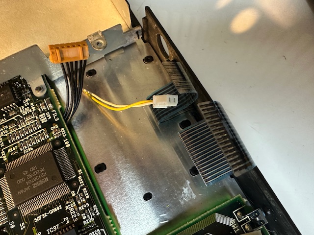
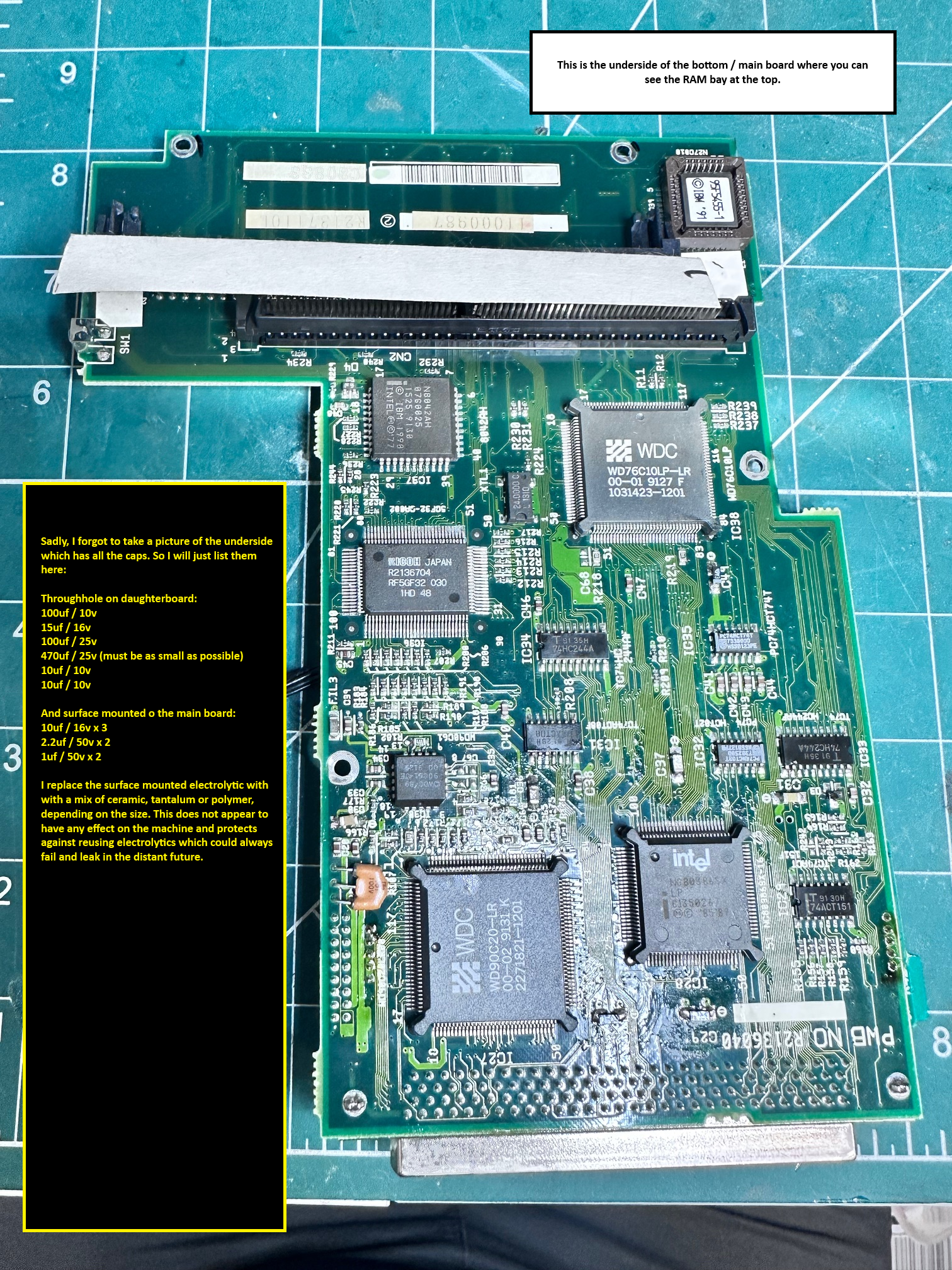
Here is the motherboard underneath:
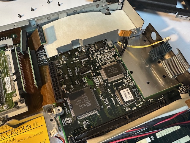
These two connectors are directly underneath the board with not a lot of space to pull them. The yellow one is (I think( for the lid detection - hibernate microswitch) and the other one possibly for the LED status lamps.
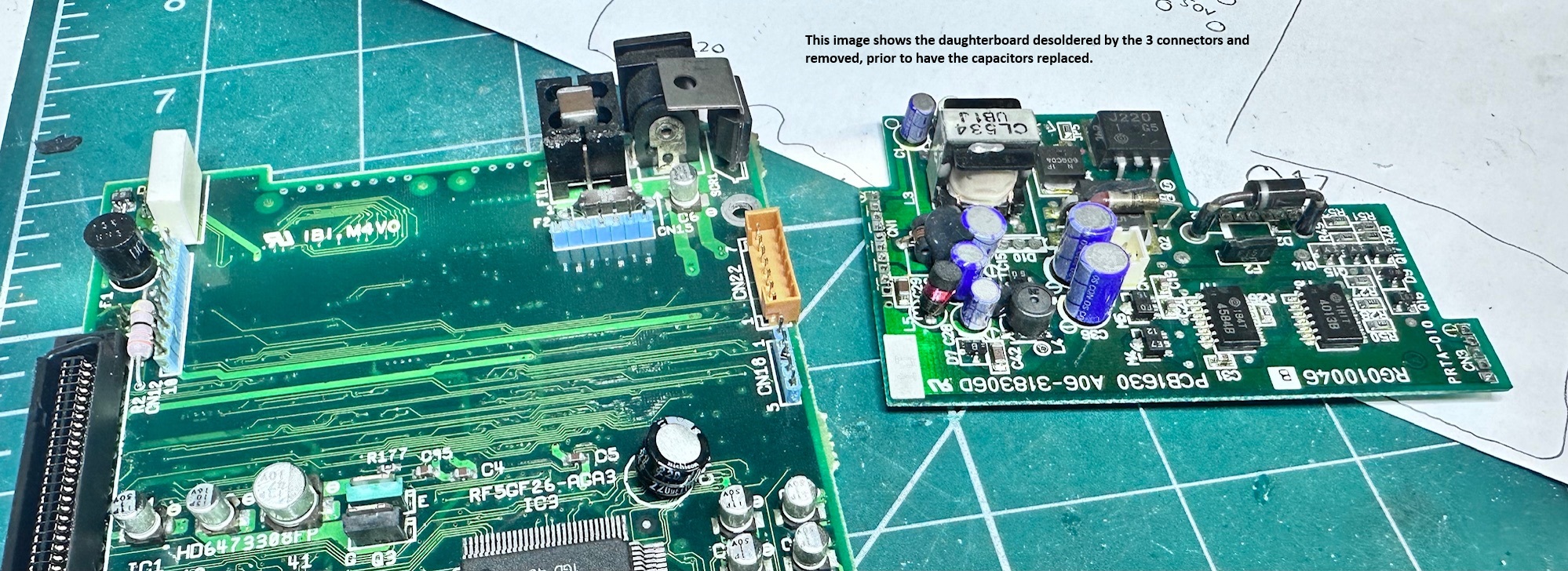
Now the hard bit - on the sub board that you have removed you'll find a daughterboard soldered on with a bunch of caps on. It's held in place by 3 soldered pin connectors, which you have to desolder to be able to remove the throughhole caps. On my removals, none of the through hole caps were leaking. Most of the surface mounted ones were.


This is the daughterboard removed. Note some of the connectors holding this daughterboard down have bridged pins. I don't know if this is intentional, but replicated the bridges when putting it back.
Here, where C11 was, it's possible the leaking electrolye had damaged some of the traces to the left of it. I can't be sure:
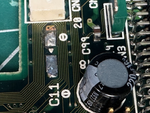
These three were definitely leaking:
And here is the recapped board, soldered back on.
Below is a picture showing the two obvious fuses. 1 is the throughole 2a fuse. Mine initially was not blown and then because I think I had an iffy barrel connector, it blew. 2) there is a strange cylinder fuse on the right - which supposedly is for the battery. Mine had not blown.
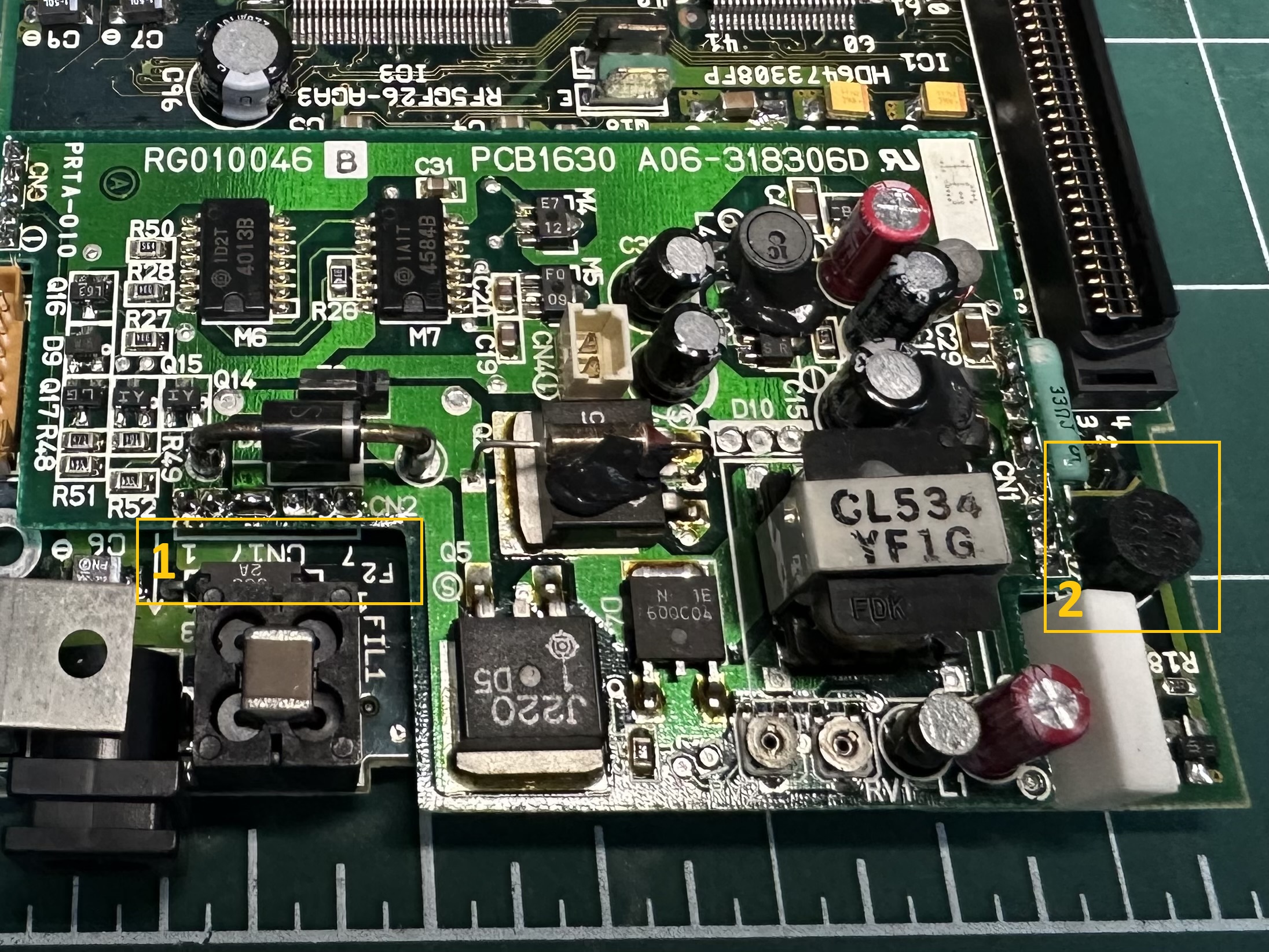
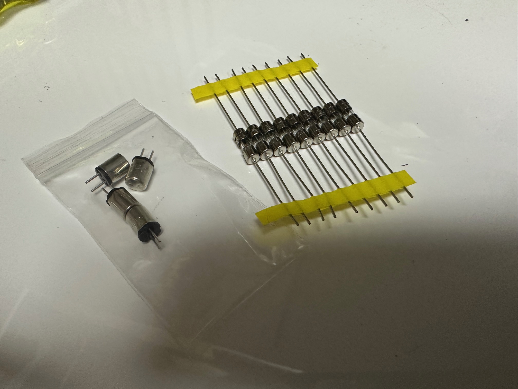
I was able to get some spare cyclinder and through-hole fuses on ebay for a few quid. I think a bundle of small 2a ones would do the trick for all 3 large fuses on the machine.
Getting the sub board back installed is a lot easier once you remove the screws around the hard drive, just to be able to pull it out. This gives you both easier access to the back connector which has to connect to the bottom of the sub board, but also the hard drive cable is quite long and gives you room to attach it before laying the board back down back into place.
IBM PS/Note N33 SX LCD / Inverter Repair
My 12Mhz N33 only could display to the internal LCD, so it was important that this worked properly. It was just about visible but something was definitely was off. These displays were bad, but not this bad and the variable resistor screen sliders wouldn't do much, apart from make the display intermittently vaguely visible and 'off'.
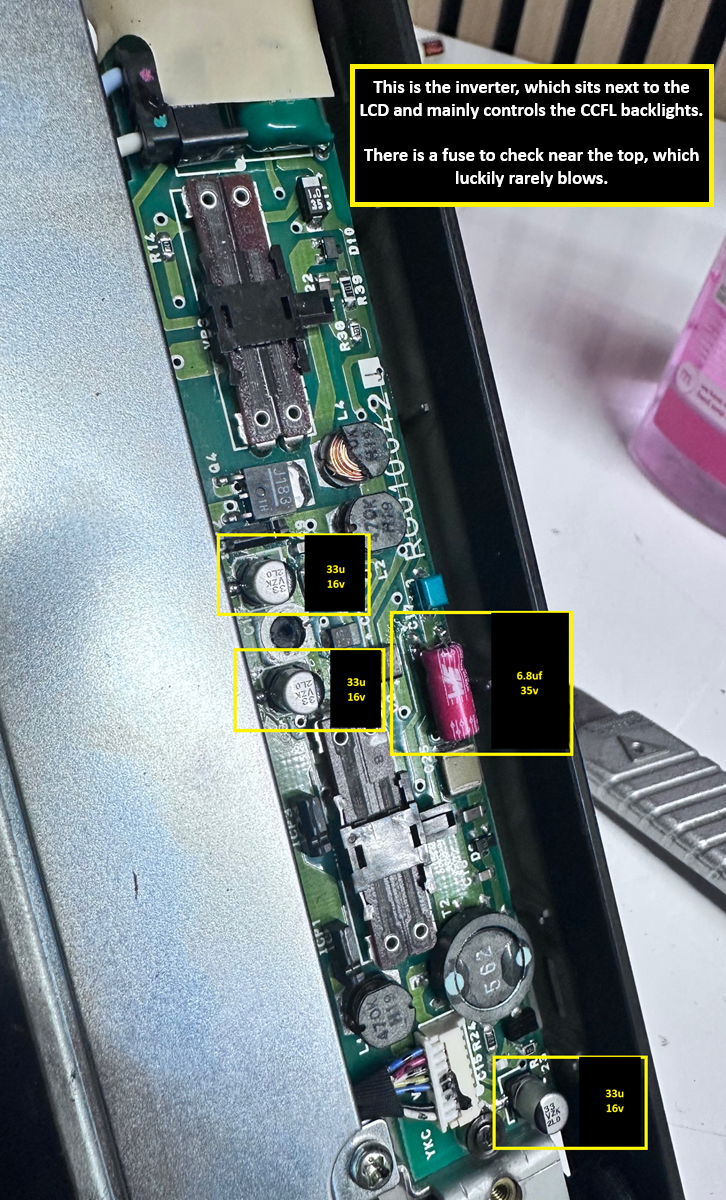
As far as I could tell, the 12Mhz and 16Mhz displays and their inverters are the same. The danger with the inverter is that it has one power connector at the top to the LCD's CCFL tube - this is generally ok. The other connector at the bottom is and 8-pin connector which has gone brittle over time. If you remove it, be very very careful as it does fall to pieces if you unplug it too many times.
As usual, capacitor were the issue and these were relatively easy to replace. You take the front panel off by removing 3 pairs of screws. 2 along the top, 2 hidden under square paper covers behind the status LEDs and another final pair behind the plastic rectangles directly above the hinges. Here's a picture in the manual showing the bottom two pairs:
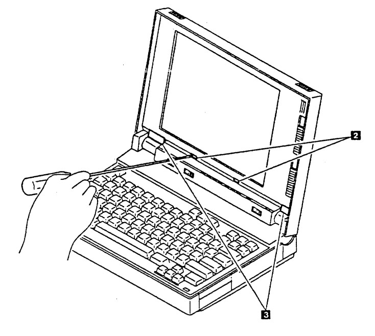
And here is with the front panel removed:
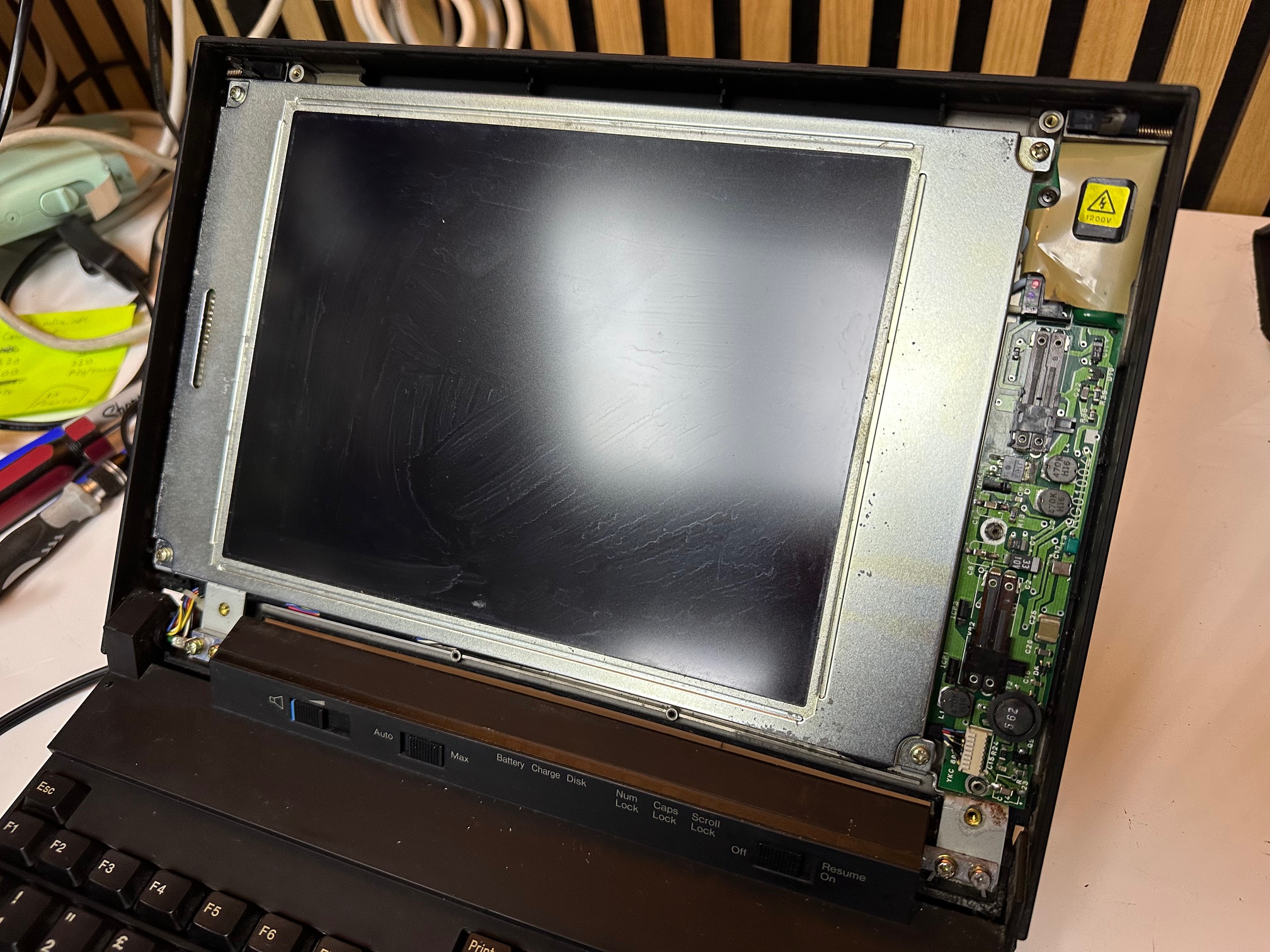
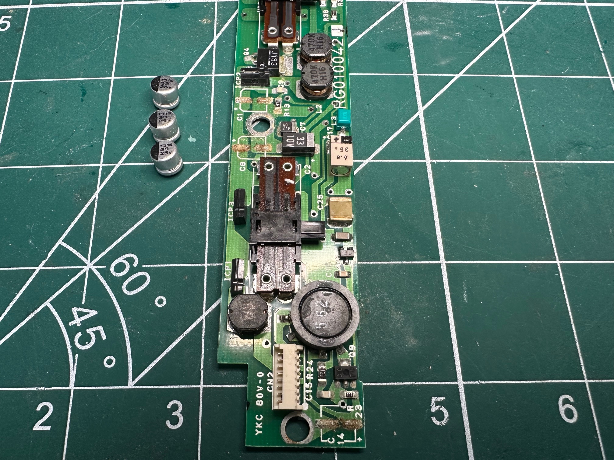
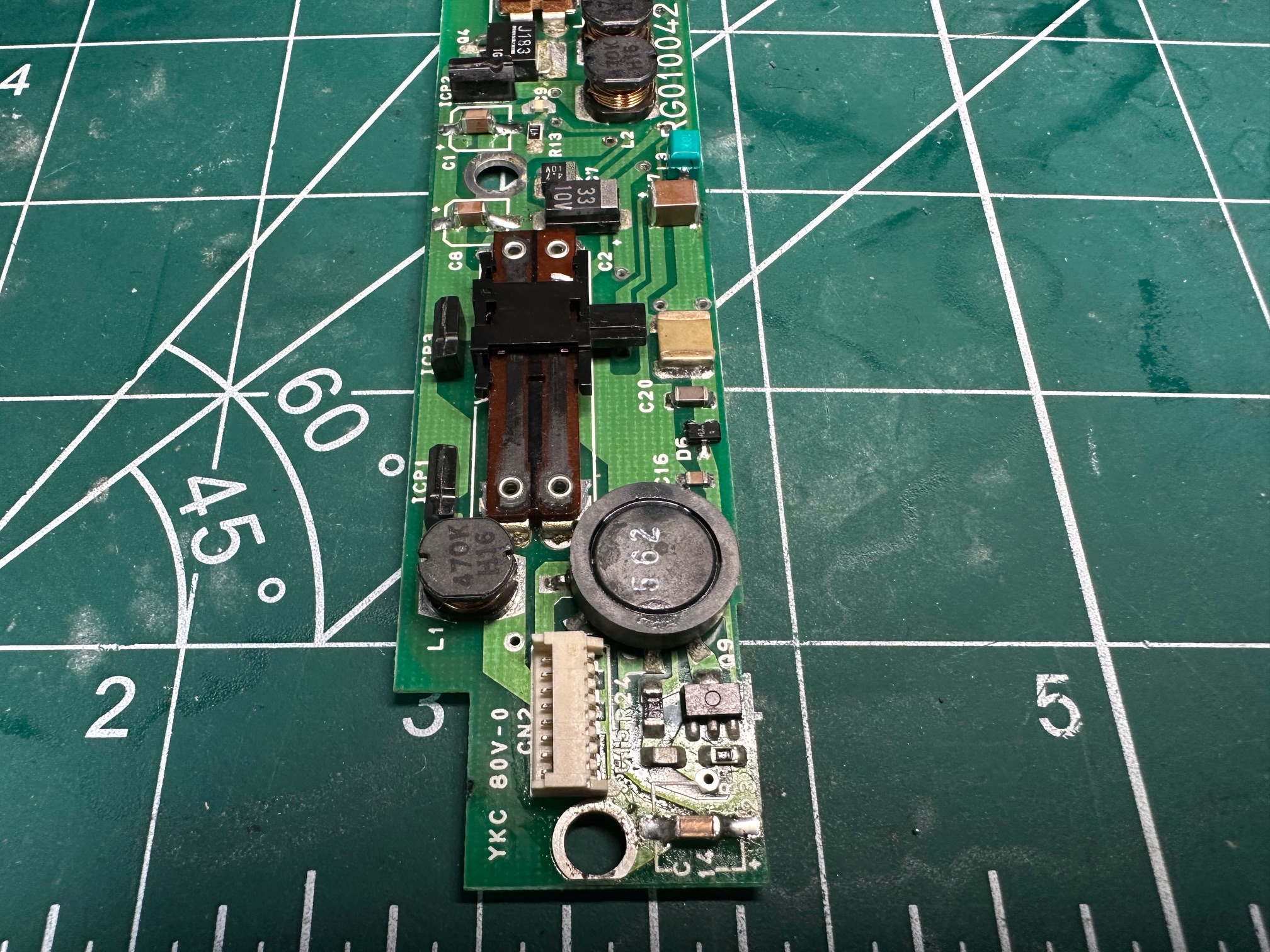
The inverter has 3 x surface mounted capacitors which are all rotten. Easily replaced with 3 ceramics. Also on the invertor is a boxed-in electrolytic measuring 6.8v. I replaced this too, because I just prefer to have no fluid caps on my machines.
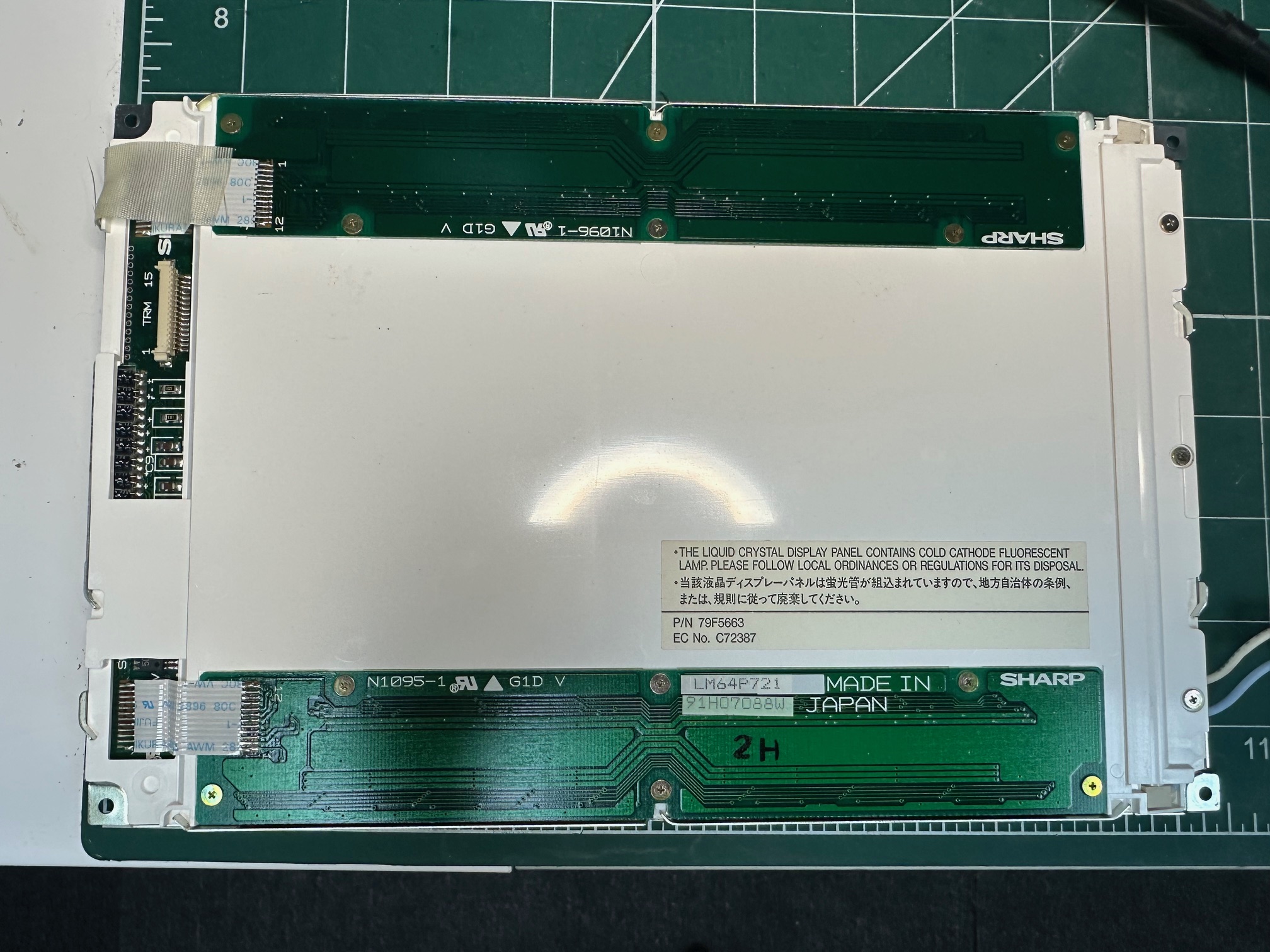
Here is the rear of the LCD panel:
Inverter Before:
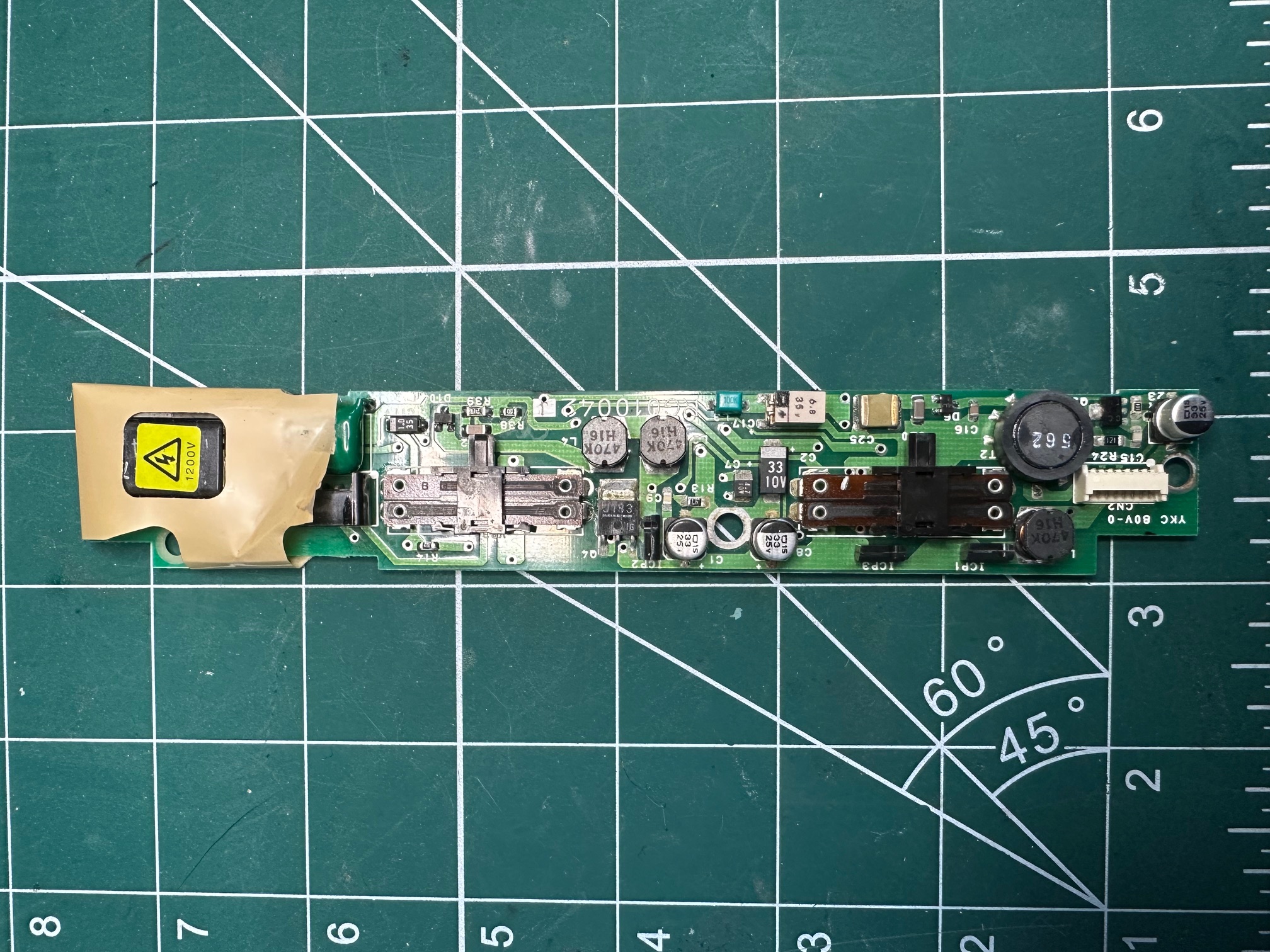
Inverter Underneath:
Inverter After:
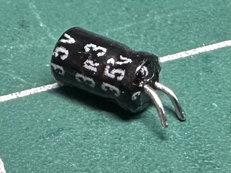
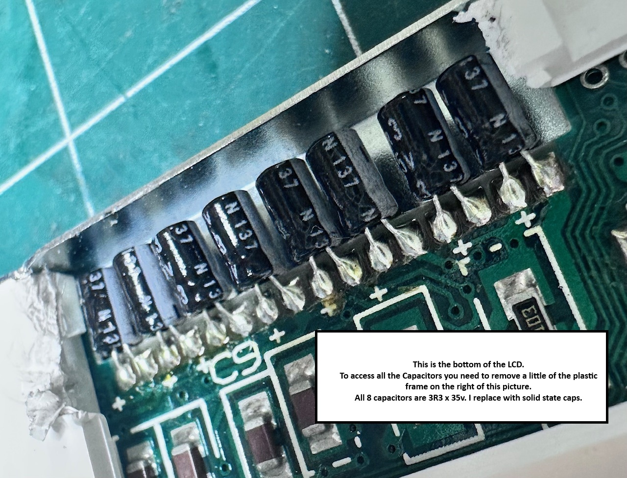
Next, the LCD itself has a row of 8 x 3R3 (0.33pf) electrolytics in a row, which I assume have failed or are failing. I replace these with tiny ceramic capacitors which seem to work fine.
This is the capacitor we're replacing:
Before Recapping:
With replaced ceramics:

N33 Floppy
The external floppy drive was old school, but only had one surface mounted electrolytic capactitor inside:


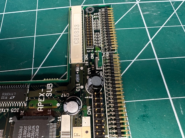
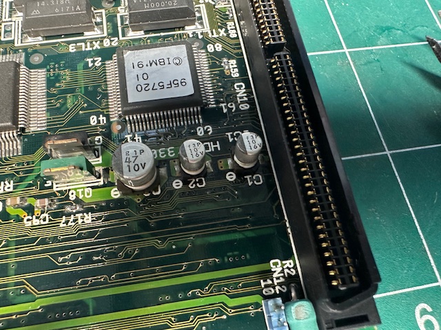
N33 APEX-MAIN Board
The second main board inside the machine has 7 surface mounted electrolytic capacitors - all of which were in the process of failing and leaving crusty residue all over the board. I replaced these with tantalums. Also on this board, close to where the main dock connector is, is a soldered on daughterboard which is held down by 5 pins either end, and on this board is 6 through-hole capacitors. None of these showed obvious signs of failure but I replaced them anyway.
Also worth noting on this soldered daughterboard, there is another through-hole 2a fuse in green.


Recovering from Lost CMOS / Dead CMOS Battery
The setup disk maker is here. You have to use the maker as copying the raw files to a floppy will not be bootable. As far as I know, these disks are not reference disks because reference disks aligned with MCA machines, not ISA machines (such as the ps/notes). However refstamping the disk doesn't seem to hurt.
The setup disk is required to restore the settings of this machine, as there is no user-configurable BIOS program built-in. The disk creator file is easy to run as long as you have an older Windows 3/95/98 machine, you can easily run this in DOS and create the disk. However I encountered another problem which I have also encountered a few times before - if one of your drives is slightly out of standard alignent, the reference disk will often not be read on a drive which didn't create it in the first place! So sometimes you may need to make the start disk on the same drive you use to boot it from - move your external floppy between machines if you can. Oddly, the nearest machine I had which matched that description was a pretty-rare 730T which immediately stepped-up and created the disk without an issue (as both machines share the same old-school IBM FDD connector, I used the same drive on both machines)
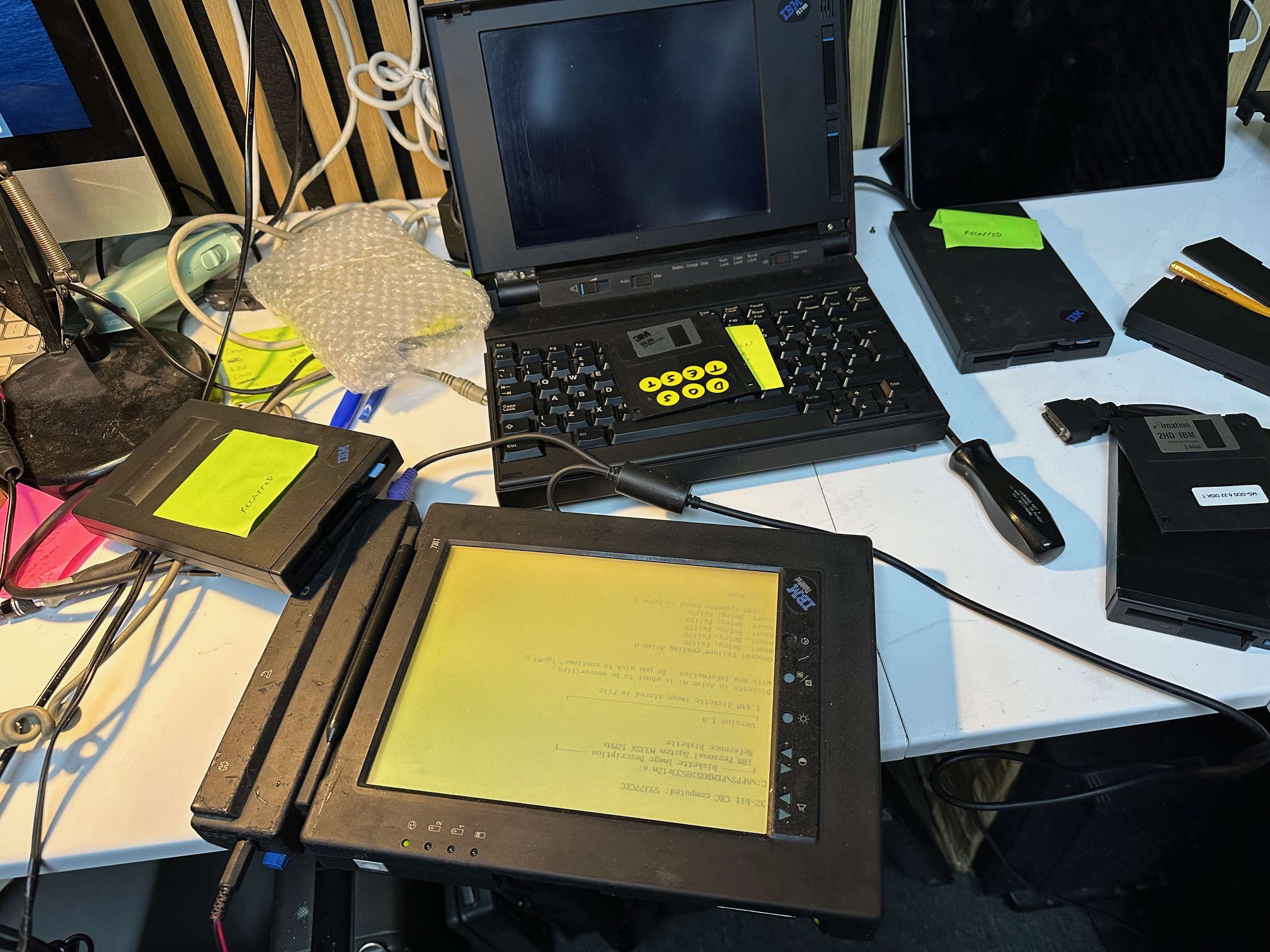
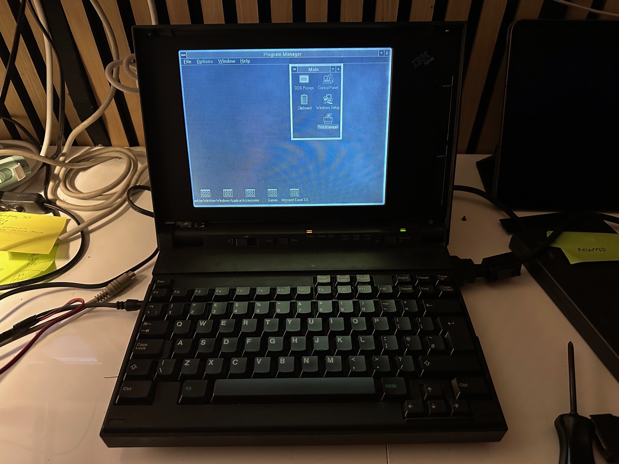
From this, I was able to plug the same floppy disk and drive back into the N33 and it booted fine, auto configured, and the hard drive booted up into DOS and Windows:
One last thing - the reference disk made on the same floppy in a different machine, worked for about 6 hours and then stopped booting. I suspect booting from floppy may eventually be this machine's downfall.
Memory / RAM
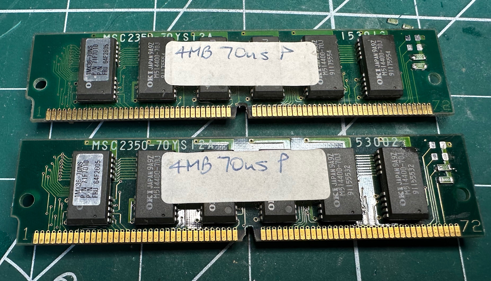
On all the ISA notes between the very first PS/55 note through to both international N33 SX machines, these machines cam with 2Mb RAM onboard, which isn't a lot. These machine's are specified as needing official 4Mb 72-pin 80NS parity RAM sticks as an upgrade. These are hard to come by and we can do better.
I managed to get four sticks of 4Mb 70ns parity 72pin simms which are faster than the required spec so would, in theory, run cooler and at lower power (not that it matters). They needed two modifications to make them work on all these ISA 12 and 16Mhz notes:
Increase the notch:
Annoyingly, the official 72-pin sticks had a bigger keyed notch in the middle than nearly all other sticks. So I used a dremel to very very slightly increase the notch size, avoiding any nearby traces in the PCB. Alternatively I could have snipped out the keying plastic inside the memory bay, but trying to preserve the machine simply means not damaging it when I don't have to.
Bridging Detect Pins
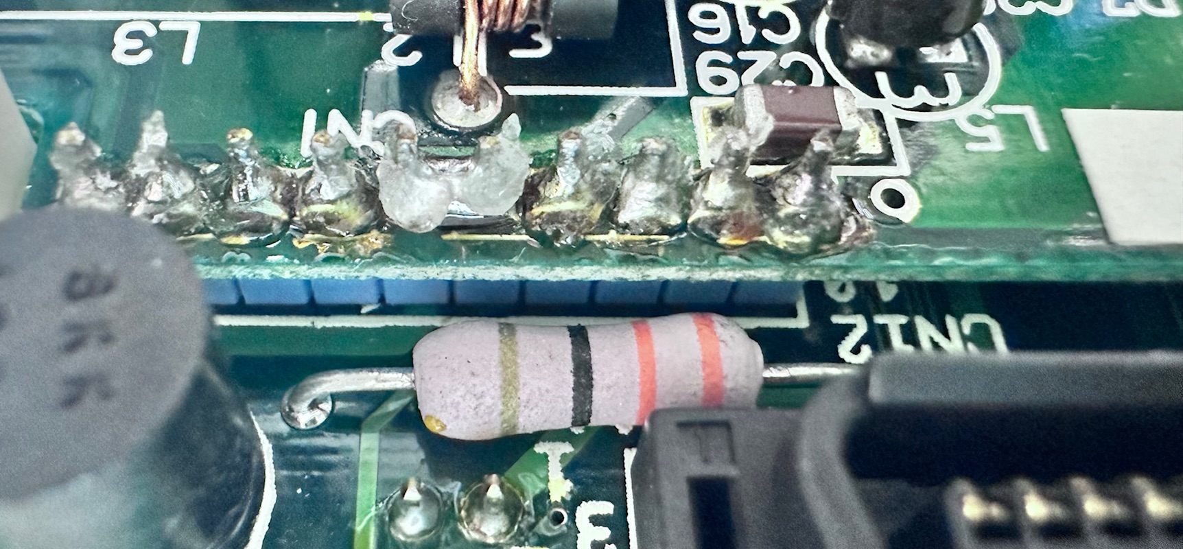
Pins 67, 68, 69 and 70 are some kind of detection/verification pin and they can either be connected to ground or not. Most sticks need modifying to make them work without getting a 225 "memory error" on power up.
In my case, the sticks I got had the wrong pins grounded, so I removed the necessary o-ohm resistors (which are essentially metal bridges) and moving them to ensure that pins 69 and 70 were grounded.
Here is a close-up of the pins on the top left corner, with top to bottom 67-68 grounded and 70 grounded:

And here is after modifying to have just 69 and 70 grounded:

On another set of RAM, I did the same but the pins were in different original positions:

And after:
CMOS
You need a working external floppy drive (with 23mm connector) and a bootable PS/note option disk to setup the machine with the right time and configure some necessary bits like the internal hard drive. I have noticed that replacing the CMOS battery with every kind available does not retain the settings beyond perhaps 1 hour. I have double checked this across various PS note machines and batteries and I've checked the voltage all the way back to the pins inside the motherboard and whilst the CMOS battery retains power to the CMOS, the settings invariably get lost. So my conclusion is that a) there is no point trying to replace the CMOS, b) You need a working floppy disk and drive to make the machine usable (otherwise it just sits on a 161/163 error) and c) if the day comes where it won't even retain it's setup on a soft boot, the notes will become entirely unsusable.
Capacitor List / Breakdown
To help people prepare for a recap, I've detailed below what capacitors are required and attached pictures where possible to help you try to determine the sizes needed. I always try and source the smallest but highess quality capacitors and only typically use RS-Online to order them. You generally pay more for smaller form factors from good brands.
A word of warning, having done these machines many times, I easily underestimate the time it takes to disassemble these machines and recap them. Knowing how to disassemble and re-assemble the 8533 PS/2 Note like the back of my hand, I can do the teardown, complete recap and reassemble and test in 6 hours. Due to the complexity of the cabling, screws and the sheer number of boards, along with the fact you have to desolder two daughterboards along the way, I would double this for your first time. In addition you should bear in mind that due to the age and type of the original solder and the amount of cleaning involved you need practice to ensure you don't damage anything. The legs on the daughterboards are particularly hard because you have to perfectly desolder on 2 or 3 edges to get it to lift off. A combination of desoldering gun (mine is set fo 840 degrees), fresh solder mixed in with the old, lots of copper braid to soak up anything the gun can't get and sometimes additional regular solderiong iron application to get it to wiggle off it whats required.
Each of the surface mounted caps are removed with snub nosed pliers, an the 'push and wiggle' technique to remove the top leaving it's legs in place to easily desolder and clean.

Here are two pictures of two of the connectors which need to be desoldered:

And here is that 1st of two daughterboards removed:
And post-recap:

And here's the bottom PCB or the second of the two:
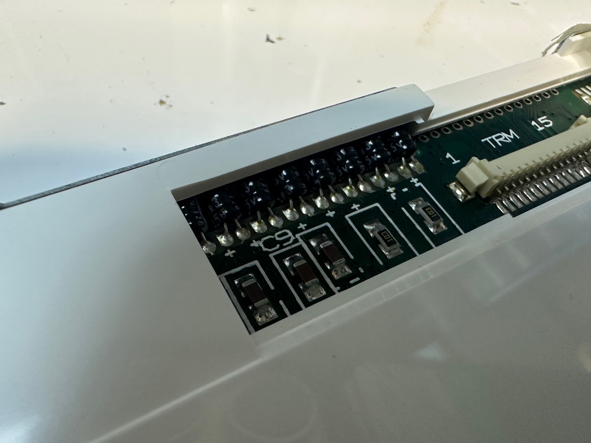
And here we have the LCD's 8 capacitors (which show no signs of failure, but I replace anyway with solid state ones (shown above)
And finally we have the Inverter:
An easy copy and paste of all the caps are listed below:
Through Hole:
4 x 220uf / 10v
3 x 10uf / 10v
2 x 4.7uf / 10v
2 x 15uf / 25v
33uf / 10v
3 x 100uf / 25v
15uf / 16v
470uf / 25v
6.8uf x 25v
Surface Mounted:
1uf / 50v
4 x 10uf / 16v
2 x 47uf / 10v
6 x 1uf / 50v
3 x 2.2uf / 50v
3 x 33uf / 16v
LCD's throughhole which I replace with Ceramic:
8 x 3.3pf / 3R3 / 35v+ surface mount
3 x 47u / 16u surface mount
1 x 6.8uf / 35v surface mount